I have heard the comparison of CPUs to brains, and while this is good for teaching the basics of computer operation, I tend to disagree with this analogy as you dive deeper into the computer hardware world. I disagree with this because a brain is made up of many parts, one of which is memory, which is a fundamental part of the operation of computer systems and biological organisms alike. That said today I am going to design a memory module for the Z80 supercomputer.
What is memory?
Understanding exactly what memory is and how it works is a fundamental part of designing computer systems. Think of memory in this case as the computers working memory, as well as its short term memory. We will use it to store variables, programs, results from computations as well any other storage that does not need to be stored after power down.
How much memory is enough?
There is no definitive answer to this question, an iPhone with 1Mb of memory would not be very useful, but a Z80 with the same would be extremely overkill. In this case, due to the memory requirements of 1024 bit numbers, which take up a whole whopping 128 bytes of memory, or .128Kb I will have around 512Kb of working memory. Due note that only one 1024 bit number wouldn't be very useful, so in order to have 256 of them we would need 32Kb of RAM, still not 512Kb but that gives me a good amount of memory for future features.
What kind of memory?
There are many kinds of memory, from the magnetic core memory used in the Apollo Guidance computer, to the NOR and NAND flash memory in the USB stick. However when talking about volatile memory, the kind used in RAM sticks and modules, SRAM and DRAM rule supreme. DRAM is expensive and generally higher capacity, however SRAM is abundant, uses less circuitry and is less expensive in smaller chip capacities. Finding memory chips with a capacity of 512Kb is not difficult, but first we need to convert to Kbits in order to make our search easier, this is a fairly easy tasks by just multiplying Kbytes by 8 to get Kbits, 512 * 8 = 4096 or 4Mbits. Another important characteristic of memory is the organization, memory comes in many different forms in order to be compatible with many different processors, in this case we need a 512x8 chip, meaning it has 512 banks of 8 bit values. The IS61C5128AL-10TLI by ISSI fits these requirements perfectly.
Wiring the chip to a Z80
Data lines
Wiring the data lines for this chip is fairly straight forward and we can follow the same general steps as the processor

Control Lines
Next up are the control lines for the memory chip, in order to address the chip properly we need to use some logic to ensure the chip is only read from during a memory read, and not an IO read, same goes for writing to the chip. This can be accomplished with a simple OR gate, since the RD/WR lines as well as the MEMRQ lines are active low, as well as the RD/WR lines on the SRAM chip.
Address Lines 0-15
Connecting these is also straightforward, its only lines 16-18 that are a tad complicated
Address Lines 16-18
Now these lines are a bit more complicated because the Z80 only has 16 bits for address space, so we need to employ some tricks to expand this address space using a technique called bank switching. In order to do this we are going to use something called a D Latch in combination with some IO logic using something called a multiplexer. However that will be built in a separate module, however for now we can add the latches using a 74hc573
The ROM
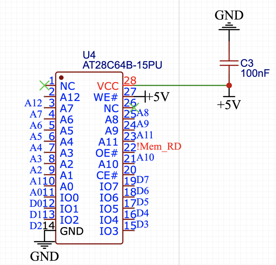
All computers need some sort of read only memory that executes immediately at startup, in this case I am going to use a 64Kbit or 8Kb, which may seem small but this can't be written to so it won't be used as RAM, for this I am going to use the at28hc64bf, This can be wired in the same way.
The #CS pin
This pin is used in order to select the memory chips we are accessing, because this chip shares memory space with the ram chip, we effectively need to disable the RAM chip when in the ROMS address space, which can be done with a ton of OR gates. And an inverter.

Placing and routing
This is the same process as last time, here is the result after using an autorouter.
What's next
There are many more boards to design, including control boards, expansion modules such as an enhanced ALU, output boards and all sorts of other boards, but I think next I will design the output board, since many of the expansion boards need to be designed before the control boards.


Top comments (0)